
Global Unichip Corp. (GUC), the advanced ASIC leader, disclosed today that it has successfully demonstrated the silicon-proven GLink (GUC multi-die interLink) interface using TSMC 7nm process and TSMC InFO_oS advanced packaging technology for AI, HPC and networking applications to do multi-die integration for system scaling.
GLink over InFO_oS is adopted due to InFO_oS cost efficiency for modular, scalable and high-yield multi-die ASICs. GLink over CoWoS is adopted by customers using multi-die ASICs with HBM memories. GLink's low area/power overhead for high throughput interconnect enables efficient multi-die InFO_oS and CoWoS solutions up to 2500mm2.
Error-free communication between dies with full duplex 0.7Tbps traffic per 1mm of beachfront, consuming just 0.25pJ/bit (0.25W per 1Tbps of full duplex traffic) was demonstrated. Testing results are fully correlated with pre-silicon simulations in all process-voltage-temperature corners. Early adopting customers are provided with detailed testing reports.
GLink's power consumption is 6-10 times lower than alternative solution using ultra-short reach SerDes-based communication through package substrate. For every 10Tbps of full duplex traffic it consumes 15-20W less power than alternative SerDes-based interface. GLink IP occupies twice less silicon area and it supports both InFO_oS and CoWoS die integration platforms.
Next generation GLink IP supporting 1.3Tbps error-free full duplex traffic per 1mm of beachfront with the same 0.25pJ/bit power consumption is already available using TSMC 5nm process. Following generation of GLink supporting 2.7Tbps/mm error-free full duplex traffic with the same 0.25pJ/bit power consumption using TSMC 5nm and 3nm process will be available during 2021. Such low power/area and traffic per beachfront efficiency makes GLink IPs perfect for AI, HPC and networking applications.
SerDes-based chips consume constant power according to absolute worst case traffic scenario. GLink-based chips consume power according to actual traffic and data pattern. SerDes-based interfaces randomize data and consume constant power according to worst case data pattern. They always consume the same amount of Watts even when traffic is reduced and data is not random. GLink parallel bus doesn't randomize data, it consumes power proportionally to actual data toggle rate and even further reduces the toggle rate using DBI. It allows our customers to consume 15-20 times less power in practical use cases than if they used SerDes-based links.
"Having a full set of best-in-class and silicon proven HBM2E/3 PHY/Controller, GLink, CoWoS and InFO_oS expertise, package design, electrical and thermal simulations, DFT and production test under one GUC roof allows our ASIC customers quick design cycle, fast bring up and production ramp up. Strong momentum of GLink adoption by our AI, HPC and networking customers supports our commitment to building wide IP portfolio and deepening GUC design expertise focusing on advanced packaging revolution" explains Dr. Ken Chen, president of GUC.
"We leveraged expertise from five generations of our HBM PHYs and Controllers in order to define a new class of high traffic density, low power, low latency, error-free GLink interfaces. We are committed to keep doubling GLink traffic density every year while keeping the same power and latency. Starting from 2021 we are going to complement HBM3 and GLink with GLink-3D bringing order of magnitude higher traffic density, order of magnitude lower latency and many times lower power using TSMC 3DFabric technology" said Igor Elkanovich, CTO of GUC.
Key highlights
- Error-free, full duplex 0.7Tbps traffic per 1mm of beachfront
- 0.25pJ/bit (i.e., 0.25W per 1Tbps of full duplex traffic)
- Testing results fully correlated with simulations in all PVT corners
- PPA advantage over SerDes/Package Substrate
1. 6-10 times lower power consumption
2. For every 10Tbps of full duplex traffic it consumes 15-20W less
3. Twice less silicon area
- GLink's low area/power overhead for high throughput interconnect enables efficient multi-die CoWoS and InFO_oS solutions up to 2500 mm2
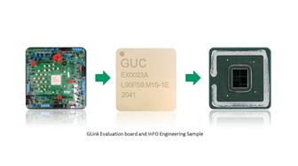
GLink evaluation board and InFO_oS engineering sample
Photo: Company
DIGITIMES' editorial team was not involved in the creation or production of this content. Companies looking to contribute commercial news or press releases are welcome to contact us.