
Connecting an application processor to a DRAM chip through a 3200 Mbps LPDDR4 interface is not any easier than routing a 2600 MHz 4G LTE antenna. While RF front ends enjoy ceramic packages and careful routing in electromagnetic proof modules, digital signals flow through ball grid array packages and small dense printed circuit boards (PCB) making them more liable to high frequency effects.
As data rates increase in the gigabit range and beyond, PCB traces can no longer be treated as simple conductors. The parasitic resistance, capacitance and inductance of the copper trace make it act as a transmission line producing all kinds of high frequency effects not commonly considered in digital design. For example, high frequency components of the signal suffer more attenuation due to skin effect than the lower frequency components causing signal deformation. The inductance and capacitance between parallel copper traces result in crosstalk and the high switching currents lead to ground bounces. Bit error rate (BER) increases as more ones become interpreted as zeros and vice versa. Hence, transmission line effects of PCB traces as well as the frequency response of packages, connecters and cables need to be thoroughly analyzed to ensure signal integrity. Accurate SPICE analysis at the PCB level can save time and cost by reducing numerous iterations of PCB prototyping and measurement.
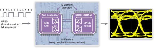
Figure 1: A typical system configuration for signal integrity analysis
Figure 1 shows a memory interface, a typical example of multi-Gigabit inter-chip communication. The same concept applies to high speed serial IO such as USB 3.0 and HDMI as well as multi-Gigabit Ethernet devices. The communication channel consists of IO models for the chips, Scattering Parameters (S-parameters) models for the packages, connectors and cables, and lossy coupled transmission line models for the PCB traces. IO models are provided by the chip vendors. Simple IO buffers can be accurately represented by IBIS models. More complex IO circuitry with active pre-emphasis and equalization are usually available in the form of encrypted transistor-level HSPICE netlists, or as IBIS-AMI models derived from the transistor-level representation. As the golden reference for transistor-level simulation, HSPICE uses foundry-certified transistor models to deliver the most accurate behavior of IO circuits. Moreover, most chip vendors use HSPICE to validate their IBIS and IBIS-AMI models. Hence using HSPICE at the board-level gives the best correlation with the chip vendor's intent. When it comes to IBIS-AMI, HSPICE has the unique capability of simulating these models in true transient mode in addition to bit by bit and statistical eye diagram modes.
Lossy coupled transmission lines for PCB traces can be extracted in different ways, the simplest of which is using HSPICE W-elements. The W-element reads in the PCB properties and the dimensions of the parallel traces, and then uses a built-in 2D solver to extract the transmission line response. The model accurately represents frequency-dependent loss and coupling, has no limit on the number of coupled lines and ensures the passivity and causality of the system. Most PCB layout tools can extract the trace geometries and automatically generate W-element models in the HSPICE netlist. Third party quasi-static 2.5D field solvers can also be used to generate broadband models of PCB traces. Depending on the field solver, these models can be inserted into the W-element in the form of RLGC tables. For critical layouts, full-wave solvers can be used to extract the frequency response of the PCB traces in the form of S-parameters which can also be used as input to the W-element.
The S-parameter models for the packages, connectors and cables are provided by the component vendor, measured by a network analyzer or extracted using a 3D electromagnetic field solver. In either case, the S-parameter model gives a robust linear representation of the component taking into account its distributed nature and any arbitrary frequency dependent behavior. Examining S-parameters on a Smith Chart gives deep insight of such distributed systems beyond what can be obtained using lumped elements in a circuit schematic. There is one challenge though. S-parameters are frequency domain models originally invented for RF and microwave devices, while signal integrity analysis of digital multi-Gigabit systems is predominantly performed in the time domain. The HSPICE S-elements overcomes this challenge using state-of-the-art automatic rational function model generation. Furthermore, HSPICE deploys multi-delay enhanced rational function models to capture the complex high frequency behavior of long data cables with several meters in length (e.g. HDMI cables). HSPICE uses parallel computing technology available in modern processors to simulate large - over 500 ports - S-parameter models with superior speed and accuracy. In addition to the use of s-parameters in circuit simulations, HSPICE also supports multiport linear network analysis (.LIN) which allows S-parameter extraction from arbitrary circuit types.
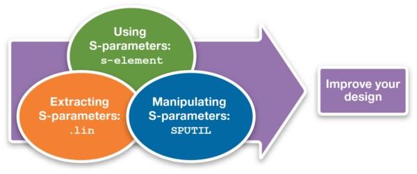
Figure 2: Working with S-parameters is more than running transient analysis
The flexibility and robustness of s-parameter modeling are sometimes compromised by the lack of quality of some s-parameter models. Low-quality S-parameter models are likely to end up with poor simulation results. Quality issues include - among other causes - passivity violation, coarse frequency sampling and narrow frequency bandwidth. For example, the starting frequency of an S-parameter model can be too high to capture low-frequency transient behavior, or the end frequency can be too low to capture the high frequency components of digital transitions. HSPICE includes a standalone S-parameter utility (SPUTIL) which can manipulate S-parameters in different ways to ensure the quality of S-parameter modeling. Figure 2 shows how HSPICE combines S-parameter extraction using multi-port linear network analysis (.LIN), S-parameter simulation using transient analysis (.TRAN) and S-parameter quality assurance using the S-parameter utility (SPUTIL).
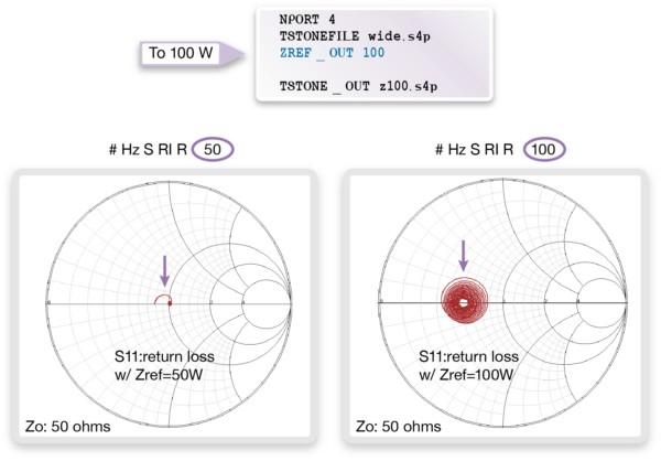
Figure 3: Checking impedance matching using HSPICE S-parameter utility (SPUTIL)
SPUTIL provides a number of convenient s-parameter manipulation techniques such as merging multiple data files, passivity checking or enforcement, re-sampling with flexible frequency point specifications, and file format conversion. For example, impedance matching is an important requirement of high speed channel design. The quickest way to test impedance matching is to observe S11 with different reference impedances. SPUTIL offers a convenient way to convert the reference impedance of a given s-parameter set using a simple script, as shown in Figure 3. Then observing the resulting S11 plot on a Smith chart and finding the smallest S11 value will give a good starting point for designing the channel termination impedance.
This concludes our discussion of the different components and models used in signal integrity analysis. Now we move to the discussion of the different analysis techniques. Eye diagram analysis is widely used for high speed communication channel evaluation. The eye diagram overlays the unit intervals of a long digital bit sequence into a compact form that readily gives picosecond-level observations of the system. Generating an eye diagram of the target system under test, examining the eye opening and measuring BER as accumulated probability are the key aspects of channel compliance testing.
HSPICE offers different techniques to analyze eye diagrams at different levels of simulation speed and accuracy. BER evaluation of multi-Gigabit systems requires the analysis of millions of unit intervals. Transient analysis of such long bit streams takes hours and produces huge data files. Thousands of simulation may be needed to cover the design space for channel optimization. Bit-by-bit and statistical eye diagram generation in HSPICE significantly improves the productivity of channel design by reducing simulation time from hours to seconds.
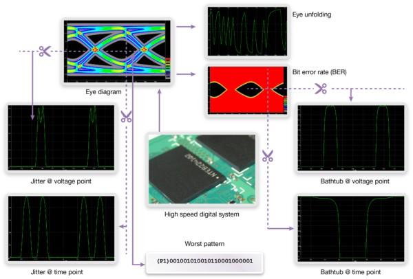
Figure 4: HSPICE statistical eye diagram analysis
HSPICE state-of-the-art statistical eye diagram analysis is applicable to all types of channels and models. HSPICE uses accurate transient analysis to calculate the impulse response of a number of small bit patterns, and then uses statistical methods to quickly generate the eye diagram as a probability density function (PDF) map that takes all the possible bit patterns into account as shown in Figure 4. HSPICE automatically extracts the jitter profiles by observing the vertical and horizontal cross sections of the eye diagram. HSPICE also generates the bit error rate (BER) map based on the PDF eye diagram. Then similarly taking cross sectional views of the BER, bathtub curves can be examined. HSPICE also captures the shortest necessary bit pattern which reproduces the inner-most - or in other terms the worst-case - eye fragment at a given time point. Using this worst bit pattern in subsequent short transient analysis, one can analyze the causes of eye closure and improve the design. HSPICE can extract time domain waveforms at particular bit positions, a useful technique for qualifying adaptive equalizer designs.
Bit-by-bit eye diagram analysis uses a fast transient technique to generate eye diagrams for specific bit patterns at a fraction of the time needed for transient analysis. Bit-by-bit and statistical eye diagram techniques are very useful for channel design. For signoff, transient analysis offers the most accurate eye diagrams. HSPICE supports all types of IO models - including algorithmic ones (IBIS-AMI) - and frequency-dependent elements in time domain transient analysis. Parallel computing technology is used to speed up the simulation of extremely long bit sequences without compromising accuracy.
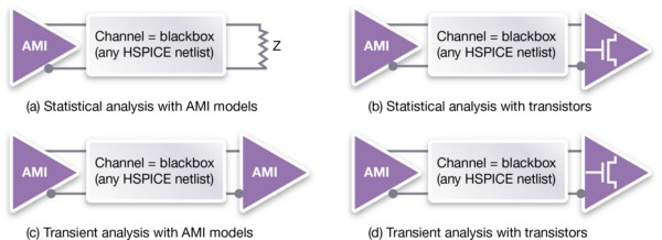
Figure 5: combining AMI and transistor-level models in statistical, bit-by-bit and transient eye diagram analysis
HSPICE has the unique ability to mix and match analysis technique and model types to best fit every stage of channel design and compliance testing. As shown in Figure 5, HSPICE treats the channel as a complete black box giving the user the option to include any combination of active and passive devices. HSPICE also allows for different transmitter and receiver representations. For example the transmitter can be a transistor level IO circuit while the receiver is an IBIS-AMI model and vice versa. In early design stages, one can use fast statistical eye diagram analysis to evaluate pattern independent transmitter emphasis. For such analysis, IBIS-AMI models are used in the transmitter side only keeping the receiver as an idealized receiver termination. Then as design evolves, one can use bit-by-bit simulation replacing the idealized receiver with an algorithmic model in order to test how well the adaptive equalizer adjusts its parameters to achieve maximum eye openings. Then by switching the analysis from bit-by-bit mode to full transient, one can capture any nonlinear effects that may happen to be in the channel. At the final verification stage, most likely full transistor representations of both transmitter and receiver buffers will be used. HSPICE has the flexibility to run all these analysis in the same testbench.
About the authors:
Hany Elhak, Product Marketing Manager, Synopsys, Inc. Elhak has more than 10 years of EDA experience spanning both technical and marketing responsibilities. Prior to EDA, Hany worked as RF designer, designing RF ICs for cellular and wireless networking standards. Hany holds B.S. and M.S. degrees in Electrical Engineering from Ain Shams University, Cairo and MBA from UC Berkeley, Haas School of Business.
Ted Mido, R&D Engineer, Synopsys, Inc. Mido is a senior staff member of HSPICE R&D group. He received the BS, MS and PhD. degrees in electrical and electronic engineering from the University of Tokyo, Japan. His researches and developments have focused on analyzing high speed signal propagation systems in analog/mixed-signal ICs, high speed chip packages and printed circuit boards. He has published numerous technical papers on interconnect analysis and parasitic extraction.

Hany Elhak
Product Marketing Manager, Synopsys, Inc.

Ted Mido
R&D Engineer, Synopsys, Inc.

