Around the web
Displaying links tagged IMEC [back to index]
17 Oct 202329 Oct 20182 Mar 201816 Nov 201713 Oct 20173 Dec 201314 Oct 201317 May 20137 Nov 20128 Oct 201223 May 20122 May 20126 Jul 201126 Oct 20109 Jun 20104 May 201012 Oct 20098 Oct 200917 Jul 200916 Oct 20086 Oct 200815 Jul 2008
The world's chipmakers are failing to meet an international target to achieve net-zero carbon emissions by 2050, experts told EE Times. The first milestone is for emissions to peak in 2025 and steadily fall, one said.
EE Times
The companies will accelerate the adoption of EUV lithography for high-volume production, including the current latest available equipment for EUV (0.33 Numerical Aperture, NA). Moreover, they will explore the potential of the next-generation high-NA EUV lithography to enable printing of even smaller nanoscale devices advancing semiconductor scaling towards the post 3nm logic node.
Company release
The tapeout project, geared toward advancing 3nm chip design, was completed using extreme ultraviolet (EUV) and 193 immersion (193i) lithography-oriented design rules and the Cadence Innovus Implementation System and Genus Synthesis Solution.
Company release
Imec has expanded its long-term joint research efforts with Western Digital. Under a new agreement, imec and Western Digital will collaborate in R&D of a broad range of advanced semiconductor technologies.
Company release
Imec and Analog Devices have entered into a strategic research partnership to develop the next generation of Internet of Things (IoT) devices.
Company release
The IMEC research center has demonstrated a new FinFET using III-V compound semiconductor material produced on 300mm wafers. This is the first time that such transistors have been produced.
Forbes
The Advanced Patterning Center will offer the global semiconductor ecosystem crucial patterning knowledge for sub-10nm technologies.
Company release
Imec and Renesas Electronics have entered into a new strategic research collaboration at Holst Centre. Together, the companies will collaborate to enhance ultra-low power (ULP) wireless technologies for short range communication, targeting sensor networks for automotive and industrial purposes.
Company release
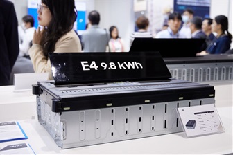
The collaboration will focus on the carbon-nanotube-based memory developed by Nantero, NRAM, and its application in high-density next-generation memories with a size under 20nm. NRAM arrays will be manufactured, tested and characterized in imec's advanced nanoelectronics facilities.
Company release
At the 2012 International Symposium on Extreme Ultraviolet Lithography, industry and research experts named the timely development of a source suited for high-volume manufacturing as the most critical issue. Other challenges remain the development of yielding masks and the further development of high-quality EUV resists.
Company release
EpiGaN NV, a startup spun out of the IMEC research institute in 2010, has officially opened a production facility for gallium nitride on silicon wafers at the Research Campus in Hasselt, Belgium.
EE Times
Company release
With a 5-year goal of manufacturing nitride-based LEDs on large-diameter silicon substrates, Siltronic has joined IMEC's gallium-nitride-on-silicon program.
LEDs Magazine
There may be 14 foreign firms approved to set up R&D centers in Taiwan this year, including those to be publicized by Elpida and Corning soon, according to the Ministry of Economic Affairs (MOEA).
CENS
Research institute IMEC has appointed Kees Den Otter, former president of TSMC Europe, to the position of vice president of emerging business.
EE Times
Hynix, IMEC, Intel, Samsung, Toshiba and possibly TSMC are the initial customers for ASML's "pre-production" extreme ultraviolet (EUV) lithography tool, according to an analyst.
EE Times
IMEC's revenues will be down only about 5% this year, compared to drops of 20% generally among electronics vendors. "R&D is the last part to cut because they need to continue to innovate," said company CEO Van den hove.
EE Times
Compound Semiconductor
MEC and JSR Corporation have collaborated on using only one etch step to reduce the cost of double patterning. 32nm lines and spaces were printed with a double exposure/single etch process, effectively freezing the resist after the first exposure. The freezing of the resist after the first exposure prevents the resist from expanding or shrinking, maintaining good CD control. When the second resist layer is added, the two do not interact.
Fabtech